Welcome to visit Hoyogo website, let's connect the world together!
Customer service hotline:+86 13723413985 or 400 058 2288
During semiconductor manufacturing, wafer inspection, metrology, and electrical testing equipment are used to evaluate wafer defects, critical process parameters, and the electrical performance of semiconductor devices, respectively. Different types of equipment vary in testing targets, signal types, and operating methods, placing different demands on signal transmission, electrical connections, and long-term operational stability. As important components of these electronic systems, PCBs provide electrical interconnections and signal transmission paths for various functional modules.
HoYoGo is a professional wafer inspection equipment PCB manufacturer with capabilities in high-reliability, high-precision, multilayer, and high-speed PCB manufacturing. To meet the requirements of wafer inspection equipment for signal transmission, circuit precision, complex interconnections, and long-term reliability, manufacturing these PCBs requires particular attention to circuit patterning, impedance control, multilayer interconnections, hole processing, and manufacturing consistency.
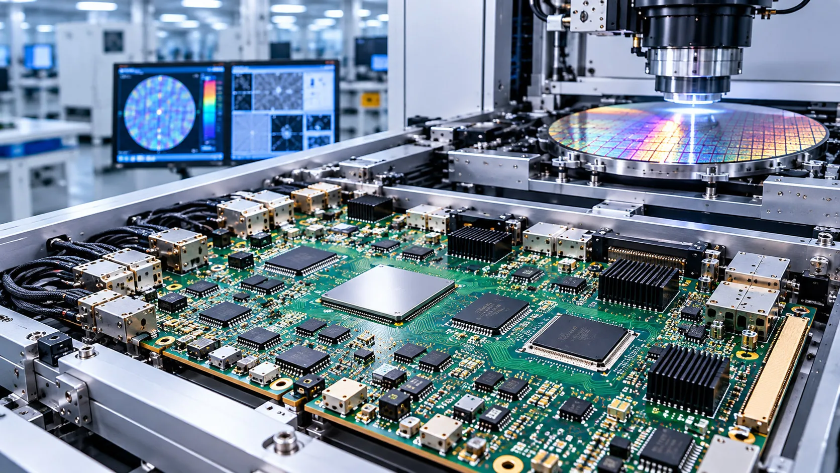
PCB Applications in Wafer Inspection Equipment
PCBs in wafer inspection equipment can be used in functional modules such as test interfaces, motion control, data acquisition, power supply, and communication, providing electrical interconnections, signal transmission paths, and power distribution for related circuits. Since equipment differs in the number of test channels, signal types, interface configurations, and system architectures, PCB materials, layer counts, stack-up structures, and interconnection designs must be determined according to specific product designs and technical requirements.
High-Precision Circuit Fabrication
Testing, data acquisition, and control circuits in wafer inspection equipment may require numerous signal and power connections within limited board space. For PCBs with high routing density, factors such as trace width, trace spacing, pad dimensions, and layer-to-layer registration accuracy can affect manufacturing quality and connection reliability.
During production, processes such as pattern transfer, etching, and layer-to-layer registration must be controlled according to customer drawings, stack-up structures, and circuit design requirements. For fine-line circuits and high-density pad areas, particular attention should be paid to trace dimensions, pad integrity, and processing uniformity to ensure that finished PCBs meet specified dimensional and electrical performance requirements.
Signal Transmission and Impedance Control
Some types of wafer inspection equipment require high-speed data acquisition and signal transmission. For controlled-impedance traces, factors such as trace width, copper thickness, dielectric thickness, and material properties can affect actual impedance. For differential pairs, trace spacing is another important parameter that requires control.
For controlled impedance PCBs, manufacturing requires control of trace dimensions, copper thickness, dielectric thickness, and related parameters according to customer-specified stack-up structures, impedance targets, and testing requirements. Controlled impedance must also be verified according to specified test methods and acceptance criteria to ensure compliance with the product's technical requirements. For certain high-speed traces, material loss characteristics and circuit fabrication consistency must also be considered according to the specific design.
Multilayer PCBs and Complex Interconnections
Wafer inspection equipment may incorporate multiple functional modules for testing, control, power distribution, data processing, and communication. For PCBs with high interconnection density, multilayer structures allow signal layers, power layers, and reference planes to be configured according to design requirements, providing routing space and interlayer connections for different circuits.
Multilayer PCB manufacturing requires careful control of inner-layer circuit fabrication, layer-to-layer registration, lamination, drilling, and hole metallization. Some high-density PCBs may also use HDI structures with microvias and other interlayer interconnection features, depending on design requirements. For these products, key manufacturing considerations include layer-to-layer registration, hole position accuracy, laser drilling quality, and hole metallization quality.
Hole Processing and Interconnection Reliability
Plated through-holes, blind vias, and microvias can provide electrical interconnections between different PCB layers. The specific hole types and interconnection methods depend on the product design. For PCBs with a large number of holes, small hole diameters, or complex interlayer connections, drilling precision, hole position accuracy, and hole metallization quality can affect interconnection reliability.
During manufacturing, drilling, electroless copper deposition, and electroplating processes must be controlled according to board thickness, hole diameter, stack-up structures, and customer technical requirements. Particular attention should be paid to the integrity and uniformity of plated copper on hole walls to reduce the risk of electrical connection failures and long-term reliability issues caused by plating defects.
PCB Reliability Under Long-Term Operating Conditions
Wafer inspection equipment generally requires stable testing and measurement performance, and some systems must operate continuously for extended periods. Electronic modules responsible for control, data processing, and power management generate heat during operation. They may also experience temperature fluctuations caused by equipment startup, shutdown, and changes in operating conditions.
Under prolonged operation and temperature variations, the thermal expansion characteristics and thermomechanical properties of PCB materials, interlayer bonding, and via interconnection quality can affect long-term stability. During manufacturing, PCB materials and manufacturing processes must be determined according to customer specifications, operating conditions, and applicable reliability requirements. Lamination quality, interlayer bonding, and plated hole quality must also be controlled to reduce the risk of reliability issues such as delamination and barrel cracking.
Manufacturing Consistency in Volume Production
Wafer inspection equipment places demanding requirements on test stability and repeatability during operation. Accordingly, PCBs used in these systems must maintain consistent manufacturing quality during volume production. Variations in material properties, dielectric thickness, trace dimensions, copper thickness, hole structures, and surface finishes can affect the dimensions and electrical performance of finished PCBs.
Throughout volume production, manufacturing processes must be controlled according to product specifications and customer technical requirements. These processes include raw material management, inner- and outer-layer circuit fabrication, lamination, drilling, electroless copper deposition, electroplating, surface finishing, and final electrical testing. Consistent process control helps ensure that finished PCBs meet the specified manufacturing and electrical performance requirements.
Development Trends in PCBs for Wafer Inspection Equipment
As semiconductor manufacturing processes and inspection requirements continue to evolve, wafer inspection equipment may need to support a wider range of test signals, higher data transmission requirements, and more complex interface connections. These evolving requirements may place greater demands on PCB manufacturing in areas such as fine-line fabrication, interlayer interconnection accuracy, and electrical performance consistency.
Different types of wafer inspection equipment vary in testing methods, channel counts, signal types, interface configurations, and system architectures. PCB materials, stack-up structures, and manufacturing processes, including circuit fabrication, must therefore be determined according to specific product specifications and customer technical requirements.
HoYoGo is a professional wafer inspection equipment PCB manufacturer with capabilities in high-reliability, high-precision, multilayer, and high-speed PCB manufacturing. To meet the requirements of wafer inspection equipment for circuit precision, complex interconnections, and long-term reliability, we provide customized PCB manufacturing services based on customer product specifications and technical requirements. Production and quality control are carried out according to applicable IPC standards and customer technical specifications, providing reliable PCB manufacturing support for wafer inspection, semiconductor testing, and related equipment.


 English
 Français
 Deutsch
 Português
 Pусский
 中文
中文