Welcome to visit Hoyogo website, let's connect the world together!
Customer service hotline:+86 13723413985 or 400 058 2288
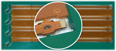
Rigid-flex PCB refers to the PCB formed by pressing the flexible PCB and rigid PCB together according to the relevant process requirements. So what is the production process of the rigid-flex board?
1. Cut Lamination: Rigid board base material cutting: Cut the large-area copper clad laminate to the size required by the design.
2. Flexible Base Material Cutting: Cut the original roll material (base material, pure glue, cover film, PI stiffener, etc.) to the size required by the design.
3. Drilling: Drill through holes for line connections.
4. Black Hole: The toner is used to make the carbon powder adhere to the hole wall, which can play a good role in connection and conduction.
5. Copper Plating: A layer of copper is plated in the hole to achieve conduction.
6. Counterpoint Explosure: Align the film (negative film) under the corresponding hole of the dry film to ensure that the film pattern can be correctly overlapped with the board surface. The film pattern is transferred to the board surface dry film through the principle of optical imaging.
7. Developing: The dry film in the unexposed area of the circuit pattern is developed by potassium carbonate or sodium carbonate, leaving the dry film pattern in the exposed area.
8. Etching: After the circuit pattern is developed, the area exposed to the copper surface is etched away by the etching solution, leaving the pattern part covered by the dry film.
9. AOI: Through the principle of optical reflection, the image is transmitted to the equipment for processing, and compared with the set data, the open and short circuit problems of the line are detected.
10.Fitting: On the copper foil circuit, cover the upper protective film to avoid oxidation or short circuit of the circuit, and at the same time play the role of insulation and product bending.
11. Lamination: The pre-stacked cover film and reinforced board are pressed into a whole through high temperature and high pressure.
12. Punching: Using the mold, the working board is punched into the shipping size that meets the customer's production and use through the power of the mechanical punching machine.
13. Fitting: Please superimpose the rigid-flex board together.
14. Lamination: Under vacuum conditions, please heat up the product gradually, and press the flexible board and rigid board together by hot pressing.
15. 2nd Drilling: Drill through hole connecting the flexible pcb and rigid pcb.
16. plasma cleaning: Use plasma to achieve effects that cannot be achieved by conventional cleaning methods.
17. Eletcroless Plating Copper(Rigid PCB): A layer of copper is plated in the hole to achieve conduction.
18. Copper Plating(rigid PCB): Use electroplating to increase the thickness of the plated through hole copper wall and the surface copper.
19. Circuit Board(Stick a dry film): Paste a layer of photosensitive material on the surface of the plated copper plate as a film for graphic transfer. Etching the AOI connection: Dissolve all the copper surfaces other than the circuit pattern to etch the required pattern.
20. Solder Mask(Silkscreen): Cover all lines and copper surfaces to protect the lines and insulation.
21. Solder Mask(Exposure): The ink will undergo a photopoly merization reaction, and the ink in the silk screen area will remain on the board and solidify.
22. Laser Decap: Use a laser cutting machine to perform laser cutting on the soft and hard cross wiring position to a certain degree, peel off the rigid board part, and expose the flexible board part.
23. Assembly: Paste steel sheet or stiffener on the corresponding area of the board surface to play the role of bonding and increase the hardness of the important parts of the FPC.
24. Testing: Use the probe to test whether there are any open/short circuit defects to ensure the product functionality.
25. Silkscreen: Marking symbols are printed on the board to facilitate the assembly and identification of subsequent products.
26. Routing: Through the CNC machine tool, the required shape can be milled according to the customer's requirements.
27. FQC: Please check the appearance of the finished products according to the customer's requirements and pick out the defective products to ensure the quality of the products.
28. Packaging: According to the customer's requirements, the qualified boards are packaged and then shipped into the warehouse.
HOYOGO is an international, professional, reliable rigid-flex PCB manufacturer. We have 2 factories production bases. Our production is strictly following high quality system of automotive products, we certified with ISO9001, ISO14001,ISO13485 and TS16949 and C-UL-S. All products strictly follow acceptance standard IPC-A-600-H and IPC-6012.


 English
 Français
 Deutsch
 Português
 Pусский
 中文
中文