Welcome to visit Hoyogo website, let's connect the world together!
Customer service hotline:+86 13723413985 or 400 058 2288
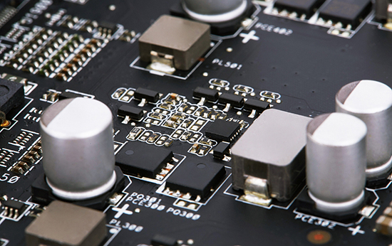
SMT package not only plays the role of placing, fixing, sealing, protecting the chip and enhancing the electrical and thermal performance, but also serves as a “bridge” between the internal circuit of the chip and the external circuit. Do you know what types of SMT package are there?
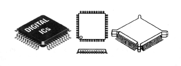
1. QFP Package
QFP package is a quad flat package, which is one of the main packaging forms of SMT integrated circuits. The leads come out from four sides in a seagull wing (L) shape. There are three types of base materials: ceramic, metal and plastic. In terms of quantity, plastic package accounts for the vast majority. When the material is not specifically indicated, in most cases it is plastic QFP.
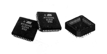
2. PLCC Package
PLCC is a plastic leaded chip carrier package for an integrated circuit. Its leads hook back inward and are called hooked (J-shaped) electrodes. Most of the integrated circuits packaged by PLCC are programmable memories. The chip can be installed on a special socket and can be easily removed to rewrite the data in it; In order to reduce the cost of the socket, the PLCC chip can also be soldered directly to the circuit board, but it is more difficult to solder by hand.
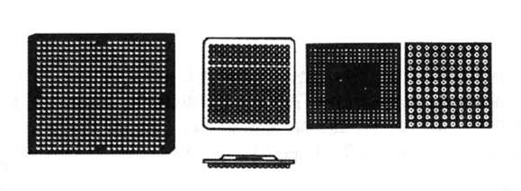
3. BGA Package
BGA package is to change the J-shaped or L-shaped leads of the original component PLCC/QFP package into ball-shaped leads. The electrodes led out in "single linear" order from around the component body are transformed into a "full plane" grid array arrangement under the bottom surface of the body. In this way, the lead spacing can be dispersed and the number of pins can be increased. BGA package has the advantages of small size and large storage space.
4. LCCC Package
LCCC has electrode pads on four sides of the ceramic substrate, and the leadless surface mount package chip is packaged on a ceramic carrier for high-speed, high-frequency integrated circuit packaging. It is characterized by a castle-like metallized groove on the side of the ceramic shell that is connected to the gold-plated electrode on the bottom of the shell. It provides a short signal path, low inductance and capacitance losses, and can be used in high-frequency working conditions, such as microprocessor unit, gate array, and memories.
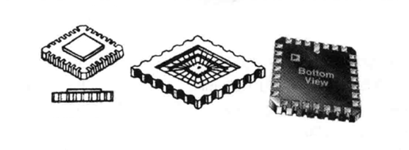

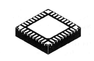
5. QFN Package
QFN is a leadless package that is square or rectangular in shape. There is a large exposed pad in the center of the bottom of the package to improve heat dissipation performance. Around the periphery of the package surrounding the large pad, there are conductive pads that make electrical connections. QFN has become an ideal choice for many new applications due to its good electrical and thermal properties, small size and light weight. QFN is very suitable for use in high-density products such as mobile phone, digital camera, PDA, DV and other portable electronic devices.
HoYoGo is an international, professional and reliable PCB manufacturer. We not only have our own factory, but we also have many years of experience in SMT processing. We can provide you with professional SMT processing service, and accept various processing forms such as customer supplied materials.


 English
 Français
 Deutsch
 Português
 Pусский
 中文
中文